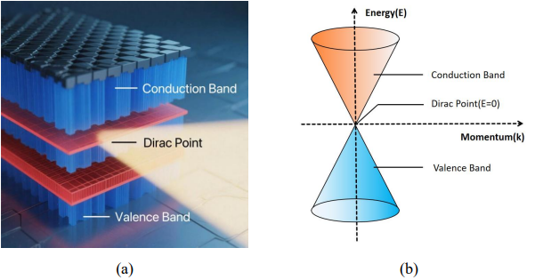
Graphene offers a promising pathway for ultra-high-speed data transmission in optical communications. Owing to its unique properties, including a zero bandgap, ultra-high carrier mobility of up to 2×105cm2V-1S-1, and strong interaction with optical fields, graphene is considered an ideal material to overcome the limitations of bandwidth, speed, and Complementary Metal-Oxide-Semiconductor (CMOS) compatibility faced by traditional electro-optic modulators. This paper first reviews the three major physical mechanisms through which graphene achieves optical modulation, the all-optical threshold switching effect brought about by saturable absorption, the Mach-Zehnder phase modulation driven by refractive index changes induced by strong light fields, and the subwavelength localization and absorption enhancement caused by the coupling of graphene and plasmas. Based on this, the paper focuses on the latest advancements in three typical graphene optical modulation devices since 2020, including the miniaturization and CMOS compatibility achieved through waveguide integration, the expansion of free-space types in optical interconnection applications, and the enhancement of plug-and-play characteristics in fiber-end types. It also elaborates on the optimization of modulation depth, insertion loss, and energy consumption in these three types of devices. Finally, the paper points out that environmental oxidation-induced performance degradation, technical bottlenecks in material transfer processes, and insufficient compatibility between large-area h-BN packaging and processes remain core challenges that restrict its large-scale industrial application.