Articles in this Volume

Research Article Open Access
Application of Semiconductor Nanomaterials in Water Pollution Treatment
Article thumbnail
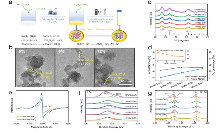
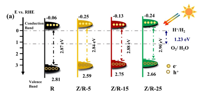
Given the rapid advancement of industrialization and urbanization, multiple forms of water pollution have grown increasingly severe. Traditional water treatment technologies face challenges such as low treatment efficiency and secondary pollution. Semiconductor nanomaterial-based photocatalysis has emerged as a promising approach for green water pollution control. This paper adopts a literature review method to systematically explore the photocatalytic water purification mechanisms of semiconductor nanomaterials, summarize four material optimization strategies and review the research progress of classical photocatalytic materials such as TiO₂, ZnO, g-C₃N₄, and Nb-doped SnO₂. Studies indicate that Nb doping introduces oxygen vacancies and synergistically modifies the band structure, significantly improving the poor visible-light response and photocorrosion susceptibility of SnO₂, while enhancing the removal efficiency for organic pollutants, heavy metals, and pathogenic bacteria. At present, this technology is limited by material stability, actual water conditions, and engineering-scale production, making large-scale implementation difficult. In the future, theoretical simulations for material optimization, immobilized catalytic devices, and supporting reactors may facilitate the transition of photocatalytic water treatment technology from laboratory research to industrial applications.
Show more
Read Article PDF
Cite
Research Article Open Access
Electrochemical Design of Semiconductor Photoelectrodes: Morphology, Interfaces, and Kinetic Bottlenecks
Article thumbnail
Photoelectrochemical conversion offers a conceptually attractive route for storing intermittent solar energy in chemical bonds, yet the practical performance of semiconductor photoelectrodes remains constrained by a well-recognized triad of losses: incomplete light harvesting, inefficient charge separation, and sluggish interfacial reaction kinetics. This invited Review examines electrochemical strategies for improving semiconductor photoelectrochemical performance, with emphasis on three representative systems: metal-assisted chemical etching of n-type silicon, cyclic voltammetry-based electrodeposition of ZnO/TiO 2 heterojunction nanorod photoanodes, and impedance spectroscopy analysis of NiO/AlGaN/n-GaN tandem photoanodes. Rather than treating these examples as isolated case studies, this Review proposes a structure-interface-kinetics framework. In this view, etching controls the optical and geometric boundary conditions of the semiconductor, electrodeposition determines the electronic quality and chemical selectivity of the surface, and impedance spectroscopy identifies the kinetic bottleneck to guide subsequent materials design. The central conclusion is that higher photocurrent density alone is not a sufficient design objective. A credible photoelectrode architecture must simultaneously preserve crystallinity, generate a beneficial interfacial field, expose kinetically competent catalytic sites, and resist corrosion under operating potentials. The Review therefore argues for an analysis-driven design philosophy in which morphology, band alignment, defect chemistry, and charge-transfer resistance are optimized as coupled variables rather than as independent descriptors.
Show more
Read Article PDF
Cite